FACILITIES
Throughout Ontario, many facilities equipped with advanced tools and instruments are available to help you to design, fabricate and test your micro- and nanoscale devices or characterize surfaces and interfaces using a variety of technique. These facilities with dedicated engineers and technician with expertise are open for business and can (conditions may apply) provide training to internal and external students, postdoctoral fellow, academic industry members. They can also provide service capabilities. Please contact them for your needs.
Nano and Microscale Nanofabrication Facilities

Waterloo Nanofab: https://uwaterloo.ca/institute-nanotechnology/
The Quantum-Nano Fabrication and Characterization Facility (QNFCF) is a core nanofabrication and characterization research facility operating under the University of Waterloo’s Office of Research. The facility includes a 6750 sq.ft. main cleanroom (with ISO 4 litho bays) located in the Mike and Ophelia Lazaridis Quantum-Nano Centre. It also includes several additional satellite labs in the QNC building as well as in the RAC1 and RAC2 buildings. This site provides information on the facility’s capabilities as well as its access, safety and operating policies. The password-protected portal includes equipment standard operating procedures as well as detailed baseline nanofabrication processes.
Giga-to-NanoElectronics Centre (G2N)
Waterloo G2N: https://uwaterloo.ca/giga-to-nanoelectronics-centre/
Established in 2005, the Centre is a hands-on facility providing users training and access to run their own research. This facility consists of groups within the University of Waterloo and external partners that make up the interdisciplinary research that spans nano-materials to large-area electronics. In addition to facilitating academic research programs, G2N also provides the capability to develop and prototype novel and emerging technologies for commercial applications.
Western nanofab: https://nanofab.uwo.ca/
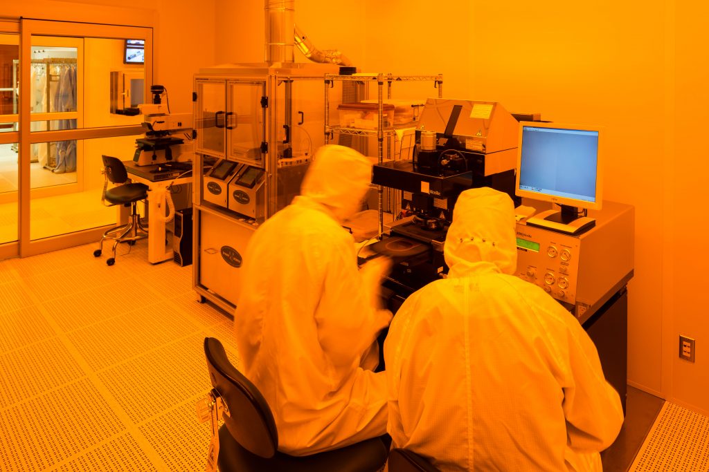
Since its inception in 2004, the open user Western Nanofabrication Facility has provided an ensemble of fabrication tools located in class 1000 and 100 clean rooms. Internal and External highly qualified personnel, postdoctoral fellows and engineers can be trained to utilize the instrumentation and fabricate their devices or image their samples in a dedicated environment. The Western Nanofabrication Facility offers dedicated tools for the fabrication of nano and micro scale features over a variety of materials such as silicon and glass. All tools in the facility are standardized for 4 inches wafers but devices can also be made on smaller samples. Lithography (UV, Nanoimprint, ebeam), thin film deposition (ebeam, magnetron sputtering, electrochemical plating, plasma enhanced chemical vapour deposition (PECVD) and osmium plasma deposition as well as 2 field-emission microscopes including one equipped with Focused ion beam are available for training or service.

Toronto Nanofab: https://tnfc.utoronto.ca/
The Toronto Nanofabrication Centre (TNFC) is an interdisciplinary research and service centre at the University of Toronto. The centre offers global research leadership by providing access to state-of-the-art nanofabrication facilities, collaborative research networks, advanced educational opportunities and information exchange events for registered users and clients. TNFC facilities are not dedicated or restricted to any particular research group. Professional staff maintain the facilities, instruct and assist users, and provide nanofabrication services for clients. TNFC facilities are open to both academic and industrial researchers, making the centre an ideal choice for open-access prototype development and testing.

Toronto Centre for advance nanotech: http://sites.utoronto.ca/ecan/index.html
Canada’s first centre for nanotechnology research, formed in September 1997 under the name The Energenius Centre for Advanced Nanotechnology (ECAN) as a result of a generous donation from Energius Inc., a Canadian company dedicated to advancing nanotechnology research. As CAN’s founding member and supporter of the Energenius Chair in Advanced Nanotechnology held by Professor Harry Ruda, Energenius entered into a strong partnership with CAN in promoting the commercialization and spin-off of nanotechnology advances to CAN and to the global market. Strong industrial support, a team of world-leading research scientists and state-of-the-art tools place CAN at the forefront for developing the key enabling technologies, nanoelectronic and nanophotonic applications, in which nanotechnology will make its first major impact – information technologies, advanced manufacturing and advanced materials and processes.

Kingston Nanofab: https://nanofabkingston.ca/
The NanoFabrication Kingston (NFK) lab began in 2015 as a collaboration between Queen’s University and CMC Microsystems, providing researchers with access to leading-edge equipment, methodologies and expertise for designing and prototyping microsystems and nanotechnologies. Since July 2019, Queen’s University is responsible for all aspects of NFK operation and management. We are an open-access lab. We provide shared tools and expertise for scientists, engineers and students from multiple disciplines, Industry. NFK has established an intellectual property (IP) framework as a guide to the various issues regarding IP rights that lab users may encounter, including IP ownership, usage rights and confidentiality. This framework encourages lab users to take into account relevant IP considerations from the outset.
Carleton University’s MicroFabrication Facility (CUMFF)
Carleton CUMFF: http://www.doe.carleton.ca/content/microfabrication-facility
Carleton University’s MicroFabrication Facility (CUMFF) is a flexible facility for manufacturing silicon integrated circuits and devices in support of research on process technology, device physics and modelling, innovative circuit techniques, photonics, biomedical devices, and microelectromechanical systems (MEMS). The facility was opened in 1993 as part of the new Minto Center for Advanced Studies in Engineering, and is the result of over 25 years of experimental research in semiconductor devices at Carleton. A notable strength of the facility is in MOS processing; MOS gate dielectrics can be produced with contamination at industrially acceptable levels. To illustrate this capability, it is worth noting that every year the CUMFF is used in a quasi-production mode to fabricate a multiproject chip in 5 micron LOCOS-isolated polysilicon gate nMOS technology containing designs submitted as a coursework project by fourth year students. These designs typically contain 50 to 100 transistors. Working chips are returned for testing within approximately three weeks of submission of CAD files, and wafer-level probing usually indicates yields of over 80% for the circuits.
Centre for Emerging Device Technologies (CEDT)
MacMaster CEDT: https://www.eng.mcmaster.ca/centre-emerging-device-technologies-cedt-0
Centre for Emerging Device Technologies (CEDT) is an organization that facilitates study of the optical, electrical, mechanical, and biological properties of semiconductors and related materials and promotes the development of technology based on these materials. The Centre’s focus has been on photonics and optical materials & devices, however, the approaches and applications are extremely diverse. Further, the research interests span a diverse area. We develop lasers, MEMS, detectors, waveguide devices, and much more. Industrial collaborations take place frequently and new initiatives are always welcome.
Surface Interface and Imaging
Surface Science Western: https://www.surfacesciencewestern.com/
Surface Science Western (SSW) is a consulting and research laboratory specializing in the analysis and characterization of surfaces and materials. The high quality, reliable analytical services provided to our clients have facilitated development and production, decreased costly returns, innovated processes and increased profitability. Since its inception in 1981, SSW has successfully served a number of high profile clients across a range of industry sectors including: energy, mineral resources, health services, automotive, aerospace, environmental, electronics and plastics. In servicing a vast range of these clients, from small manufacturing facilities to industrial giants, SSW has garnered a solid reputation for quality, innovation and timely service. Along with the 250 people-years of experience and unparalleled interpretive skills of our researchers, SSW is also one of Canada’s best-equipped laboratories for surface and materials analysis. An ISO 9001:2015 lab, located at The University of Western Ontario in London, Ontario, SSW provides clients with direct and convenient access to a number of highly skilled and experienced professionals who are committed to improving quality using state-of-the-art analytical techniques.
MacMaster CCEM: https://ccem.mcmaster.ca/
The Canadian Centre for Electron Microscopy provides world-class electron microscopy capabilities and expertise to Canadian researchers and industry working in a broad range of fields. Our vision is to be one of the leading electron microscopy facilities in the world for the quality of the scientific research, to be the go-to provider of electron microscopy services to Canadian industry and to play a leading role in promoting interactions amongst researchers in various fields nationally and internationally. Located at McMaster University and operated by the Brockhouse Institute for Materials Research, the CCEM features a state-of-the-art suite of instrumentation and experienced, dedicated staff capable of getting the best out of each instrument. We are happy to work with you to find solutions to your materials research and development questions.
Carleton Imaging facility: http://nif.carleton.ca/
The Carleton Nano Imaging Facility (NIF) is home to two state-of-the-art Electron Microscopes, Tescan VegaII XMU SEM and FEI Tecnai G2 TEM. The tungsten Tescan VegaII SEM images specimen surface profiles and topographies at variable pressures. It is operational at high vacuum for maximum resolution or low vacuum for direct imaging of fresh unprocessed biological specimens. It is equipped with Oxford X-ray detection systems (INCA EDS) for elemental analysis and quantitative mapping. A Cryo stage is also available for the low-temperature operation. The FEI Tecnai G2 TEM reveals specimen information down to the atomic level where it reaches a stunning 1-million magnification. The FEI Tecnai G2 features a field emission source which makes the ultra-high resolution imaging possible – a spatial resolution as small as 0.144nm can be achieved. The Tecnai G2 is equipped with the latest Oxford X-ray detection systems – Aztec EDS which offers high-degree accuracy at a fast data acquisition speed. Our staffs at the Carleton Nano Imaging Facility are available to assist users at all levels of expertise. We offer a full spectrum of technical support that ranges from training courses, to sample preparation, to instrument operation and energy dispersive x-ray analysis. Academic, government, and commercial users are welcome to take advantage of our expertise.
Interface Science Western
Interface Science Western: http://isw.physics.uwo.ca/
Interface Science Western is the home of the Tandetron Accelerator Facility, a part of the Canadian Charged Particle Accelerator Consortium (CCPAC). This is a National Facility supported in part by an NSERC Major Research Support grant. ISW allows users to undertake a broad range of materials research projects using ion beam analysis and ion implantation. Ion implantation is the process by which impurities are introduced into semiconductors to create microelectronic devices, and so is one of the key techniques that makes fast computers and smartphones possible. ISW has extensive materials characterization and processing capabilities available to users.
Waterloo Advanced Technology Laboratory (Watlab)
Waterloo Advanced Technology Laboratory (Watlab): http://leung.uwaterloo.ca/watlab/
Established with funding support from Canada Foundation for Innovation and the Province of Ontario in 1999, WATLab is the first multidisciplinary materials research centre in Canada’s Technology Triangle. WATLab offers a completetoolset for advanced materials research and emerging technology development. We offer pay-per-use service for both academic and industrial users at competitive rates, with our expert operators providing sample characterization measurement (and analysis). For a selected number of tools (e.g. SEM), we also provide training to allow the users to access the tools through a self-serve booking system.
Materials Facilities
Fraunhofer-Western University Project Centre for Composite Research
Fraunhofer-Western University Project Centre for Composite Research: https://www.eng.uwo.ca/fraunhofer/
The Fraunhofer Project Centre for Composites Research is a joint venture between Western University and the Fraunhofer Institute of Chemical Technology (ICT) in Pfinztal, Germany. The FPC @ Western develops, tests, validates and characterizes new lightweight materials and advanced manufacturing processes at industrial scale. By combining Fraunhofer’s latest global technologies and Western’s strengths in materials engineering, the FPC @ Western proactively addresses the needs of its industry partners.
Centre for Advanced Materials Joining: https://uwaterloo.ca/centre-advanced-materials-joining/
The primary goal of the Centre for Advanced Materials Joining (CAMJ) at the University of Waterloo, Ontario, Canada is to develop new and innovative technologies for materials joining. CAMJ has cutting-edge laboratory facilities and research areas to collaborate with leading companies in the industry for research and development. CAMJ trains students on the undergraduate, masters, PhD, and postdoctoral levels and collaborates with students from foreign institutes of excellence to extend their research. The projects taken up in CAMJ in the areas of micro-welding, micro and nano-joining, laser, arc, resistance and friction stir welding that can be utilized towards a variety of applications in medical, nanomechatronics, wire bonding and automotive and aerospace applications.
Toronto Metropolitan Analytical Center

Toronto Metropolitan Analytical Center: https://www.torontomu.ca/analytical-centre/
The Toronto Metropolitan Analytical Centre (TMAC) is a state-of-the-art facility that houses a wide range of equipment that is open to the TMU community as well as to external companies looking for testing of their products. Resources include a full suite of spectroscopy, chromatography, and elemental analysis. We can also perform powder x-ray diffraction, and both differential scanning calorimetry and thermal gravimetric analysis.
Throughout Ontario, many facilities equipped with advanced tools and instruments are available to help you to design, fabricate and test your micro- and nanoscale devices or characterize surfaces and interfaces using a variety of technique. These facilities with dedicated engineers and technician with expertise are open for business and can (conditions may apply) provide training to internal and external students, postdoctoral fellow, academic industry members. They can also provide service capabilities. Please contact them for your needs.
Nano and Microscale Nanofabrication Facilities
Waterloo Nanofab: https://uwaterloo.ca/institute-nanotechnology/
The Quantum-Nano Fabrication and Characterization Facility (QNFCF) is a core nanofabrication and characterization research facility operating under the University of Waterloo’s Office of Research. The facility includes a 6750 sq.ft. main cleanroom (with ISO 4 litho bays) located in the Mike and Ophelia Lazaridis Quantum-Nano Centre. It also includes several additional satellite labs in the QNC building as well as in the RAC1 and RAC2 buildings. This site provides information on the facility’s capabilities as well as its access, safety and operating policies. The password-protected portal includes equipment standard operating procedures as well as detailed baseline nanofabrication processes.
Giga-to-NanoElectronics
Centre (G2N)
Waterloo G2N: https://uwaterloo.ca/giga-to-nanoelectronics-centre/
Established in 2005, the Centre is a hands-on facility providing users training and access to run their own research. This facility consists of groups within the University of Waterloo and external partners that make up the interdisciplinary research that spans nano-materials to large-area electronics. In addition to facilitating academic research programs, G2N also provides the capability to develop and prototype novel and emerging technologies for commercial applications.
Western nanofab: https://nanofab.uwo.ca/
Since its inception in 2004, the open user Western Nanofabrication Facility has provided an ensemble of fabrication tools located in class 1000 and 100 clean rooms. Internal and External highly qualified personnel, postdoctoral fellows and engineers can be trained to utilize the instrumentation and fabricate their devices or image their samples in a dedicated environment. The Western Nanofabrication Facility offers dedicated tools for the fabrication of nano and micro scale features over a variety of materials such as silicon and glass. All tools in the facility are standardized for 4 inches wafers but devices can also be made on smaller samples. Lithography (UV, Nanoimprint, ebeam), thin film deposition (ebeam, magnetron sputtering, electrochemical plating, plasma enhanced chemical vapour deposition (PECVD) and osmium plasma deposition as well as 2 field-emission microscopes including one equipped with Focused ion beam are available for training or service.
Toronto Nanofab: https://tnfc.utoronto.ca/
The Toronto Nanofabrication Centre (TNFC) is an interdisciplinary research and service centre at the University of Toronto. The centre offers global research leadership by providing access to state-of-the-art nanofabrication facilities, collaborative research networks, advanced educational opportunities and information exchange events for registered users and clients. TNFC facilities are not dedicated or restricted to any particular research group. Professional staff maintain the facilities, instruct and assist users, and provide nanofabrication services for clients. TNFC facilities are open to both academic and industrial researchers, making the centre an ideal choice for open-access prototype development and testing.
Toronto Centre for advance nanotech: http://sites.utoronto.ca/ecan/index.html
Canada’s first centre for nanotechnology research, formed in September 1997 under the name The Energenius Centre for Advanced Nanotechnology (ECAN) as a result of a generous donation from Energius Inc., a Canadian company dedicated to advancing nanotechnology research. As CAN’s founding member and supporter of the Energenius Chair in Advanced Nanotechnology held by Professor Harry Ruda, Energenius entered into a strong partnership with CAN in promoting the commercialization and spin-off of nanotechnology advances to CAN and to the global market. Strong industrial support, a team of world-leading research scientists and state-of-the-art tools place CAN at the forefront for developing the key enabling technologies, nanoelectronic and nanophotonic applications, in which nanotechnology will make its first major impact – information technologies, advanced manufacturing and advanced materials and processes.
Kingston Nanofab: https://nanofabkingston.ca/
The NanoFabrication Kingston (NFK) lab began in 2015 as a collaboration between Queen’s University and CMC Microsystems, providing researchers with access to leading-edge equipment, methodologies and expertise for designing and prototyping microsystems and nanotechnologies. Since July 2019, Queen’s University is responsible for all aspects of NFK operation and management. We are an open-access lab. We provide shared tools and expertise for scientists, engineers and students from multiple disciplines, Industry. NFK has established an intellectual property (IP) framework as a guide to the various issues regarding IP rights that lab users may encounter, including IP ownership, usage rights and confidentiality. This framework encourages lab users to take into account relevant IP considerations from the outset.
Carleton University’s MicroFabrication Facility (CUMFF)
Carleton CUMFF: http://www.doe.carleton.ca/content/microfabrication-facility
Carleton University’s MicroFabrication Facility (CUMFF) is a flexible facility for manufacturing silicon integrated circuits and devices in support of research on process technology, device physics and modelling, innovative circuit techniques, photonics, biomedical devices, and microelectromechanical systems (MEMS). The facility was opened in 1993 as part of the new Minto Center for Advanced Studies in Engineering, and is the result of over 25 years of experimental research in semiconductor devices at Carleton. A notable strength of the facility is in MOS processing; MOS gate dielectrics can be produced with contamination at industrially acceptable levels. To illustrate this capability, it is worth noting that every year the CUMFF is used in a quasi-production mode to fabricate a multiproject chip in 5 micron LOCOS-isolated polysilicon gate nMOS technology containing designs submitted as a coursework project by fourth year students. These designs typically contain 50 to 100 transistors. Working chips are returned for testing within approximately three weeks of submission of CAD files, and wafer-level probing usually indicates yields of over 80% for the circuits.
Centre
for Emerging Device Technologies (CEDT)
MacMaster CEDT: https://www.eng.mcmaster.ca/centre-emerging-device-technologies-cedt-0
Centre for Emerging Device Technologies (CEDT) is an organization that facilitates study of the optical, electrical, mechanical, and biological properties of semiconductors and related materials and promotes the development of technology based on these materials. The Centre’s focus has been on photonics and optical materials & devices, however, the approaches and applications are extremely diverse. Further, the research interests span a diverse area. We develop lasers, MEMS, detectors, waveguide devices, and much more. Industrial collaborations take place frequently and new initiatives are always welcome.
Surface Interface and Imaging
Surface Science Western: https://www.surfacesciencewestern.com/
Surface Science Western (SSW) is a consulting and research laboratory specializing in the analysis and characterization of surfaces and materials. The high quality, reliable analytical services provided to our clients have facilitated development and production, decreased costly returns, innovated processes and increased profitability. Since its inception in 1981, SSW has successfully served a number of high profile clients across a range of industry sectors including: energy, mineral resources, health services, automotive, aerospace, environmental, electronics and plastics. In servicing a vast range of these clients, from small manufacturing facilities to industrial giants, SSW has garnered a solid reputation for quality, innovation and timely service. Along with the 250 people-years of experience and unparalleled interpretive skills of our researchers, SSW is also one of Canada’s best-equipped laboratories for surface and materials analysis. An ISO 9001:2015 lab, located at The University of Western Ontario in London, Ontario, SSW provides clients with direct and convenient access to a number of highly skilled and experienced professionals who are committed to improving quality using state-of-the-art analytical techniques.
MacMaster CCEM: https://ccem.mcmaster.ca/
The Canadian Centre for Electron Microscopy provides world-class electron microscopy capabilities and expertise to Canadian researchers and industry working in a broad range of fields. Our vision is to be one of the leading electron microscopy facilities in the world for the quality of the scientific research, to be the go-to provider of electron microscopy services to Canadian industry and to play a leading role in promoting interactions amongst researchers in various fields nationally and internationally. Located at McMaster University and operated by the Brockhouse Institute for Materials Research, the CCEM features a state-of-the-art suite of instrumentation and experienced, dedicated staff capable of getting the best out of each instrument. We are happy to work with you to find solutions to your materials research and development questions.
Carleton Imaging facility: http://nif.carleton.ca/
The Carleton Nano Imaging Facility (NIF) is home to two state-of-the-art Electron Microscopes, Tescan VegaII XMU SEM and FEI Tecnai G2 TEM. The tungsten Tescan VegaII SEM images specimen surface profiles and topographies at variable pressures. It is operational at high vacuum for maximum resolution or low vacuum for direct imaging of fresh unprocessed biological specimens. It is equipped with Oxford X-ray detection systems (INCA EDS) for elemental analysis and quantitative mapping. A Cryo stage is also available for the low-temperature operation. The FEI Tecnai G2 TEM reveals specimen information down to the atomic level where it reaches a stunning 1-million magnification. The FEI Tecnai G2 features a field emission source which makes the ultra-high resolution imaging possible – a spatial resolution as small as 0.144nm can be achieved. The Tecnai G2 is equipped with the latest Oxford X-ray detection systems – Aztec EDS which offers high-degree accuracy at a fast data acquisition speed. Our staffs at the Carleton Nano Imaging Facility are available to assist users at all levels of expertise. We offer a full spectrum of technical support that ranges from training courses, to sample preparation, to instrument operation and energy dispersive x-ray analysis. Academic, government, and commercial users are welcome to take advantage of our expertise.
Interface
Science Western
Interface Science Western: http://isw.physics.uwo.ca/
Interface Science Western is the home of the Tandetron Accelerator Facility, a part of the Canadian Charged Particle Accelerator Consortium (CCPAC). This is a National Facility supported in part by an NSERC Major Research Support grant. ISW allows users to undertake a broad range of materials research projects using ion beam analysis and ion implantation. Ion implantation is the process by which impurities are introduced into semiconductors to create microelectronic devices, and so is one of the key techniques that makes fast computers and smartphones possible. ISW has extensive materials characterization and processing capabilities available to users.
Waterloo Advanced
Technology Laboratory (Watlab)
Waterloo Advanced Technology Laboratory (Watlab): http://leung.uwaterloo.ca/watlab/
Established with funding support from Canada Foundation for Innovation and the Province of Ontario in 1999, WATLab is the first multidisciplinary materials research centre in Canada’s Technology Triangle. WATLab offers a completetoolset for advanced materials research and emerging technology development. We offer pay-per-use service for both academic and industrial users at competitive rates, with our expert operators providing sample characterization measurement (and analysis). For a selected number of tools (e.g. SEM), we also provide training to allow the users to access the tools through a self-serve booking system.
Materials Facilities
Fraunhofer-Western
University Project Centre for Composite Research
Fraunhofer-Western University Project Centre for Composite Research: https://www.eng.uwo.ca/fraunhofer/
The Fraunhofer Project Centre for Composites Research is a joint venture between Western University and the Fraunhofer Institute of Chemical Technology (ICT) in Pfinztal, Germany. The FPC @ Western develops, tests, validates and characterizes new lightweight materials and advanced manufacturing processes at industrial scale. By combining Fraunhofer’s latest global technologies and Western’s strengths in materials engineering, the FPC @ Western proactively addresses the needs of its industry partners.
Centre for Advanced Materials Joining: https://uwaterloo.ca/centre-advanced-materials-joining/
The primary goal of the Centre for Advanced Materials Joining (CAMJ) at the University of Waterloo, Ontario, Canada is to develop new and innovative technologies for materials joining. CAMJ has cutting-edge laboratory facilities and research areas to collaborate with leading companies in the industry for research and development. CAMJ trains students on the undergraduate, masters, PhD, and postdoctoral levels and collaborates with students from foreign institutes of excellence to extend their research. The projects taken up in CAMJ in the areas of micro-welding, micro and nano-joining, laser, arc, resistance and friction stir welding that can be utilized towards a variety of applications in medical, nanomechatronics, wire bonding and automotive and aerospace applications.
Toronto Metropolitan Analytical Centre
Toronto Metropolitan Analytical Center: https://www.torontomu.ca/analytical-centre/
The Toronto Metropolitan Analytical Centre (TMAC) is a state-of-the-art facility that houses a wide range of equipment that is open to the TMU community as well as to external companies looking for testing of their products. Resources include a full suite of spectroscopy, chromatography, and elemental analysis. We can also perform powder x-ray diffraction, and both differential scanning calorimetry and thermal gravimetric analysis.
Technical Specialists are on hand to provide training and assist with method development for your samples. This facility is located within the Faculty of Science at Toronto Metropolitan University in downtown Toronto, has 24/7 access and competitive rates for your analytical needs.
Please reach out via our contact page for any questions or inquiries.
A trusted source of information for all nanoscience and nanotechnology activity in Ontario.